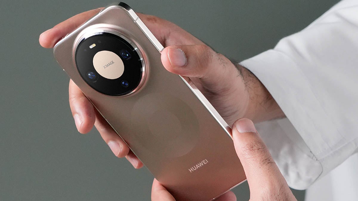

BEIJING – Somewhere in the Oregon clean room where SemiAnalysis runs its new Teardown Engineering and Evaluation Lab, a researcher slid a Huawei Mate 80 Pro Max under a transmission electron microscope and confirmed what the headline will not tell you. The story of the Kirin 9030 is not about metal pitch. It is about memory.
When SemiAnalysis published its first public teardown report on June 14 – the chip industry’s most anticipated physical analysis of the year – the finding that traveled fastest was a number: SMIC’s N+3 node has a minimum local metal pitch of 32.5 nanometers, narrower than the 36-nanometer pitch shipping in Intel’s Panther Lake CPUs on its 18A process. That comparison spread across semiconductor forums within hours. SemiAnalysis, for its part, called it a cherry-picked metric in the second paragraph of its own report.
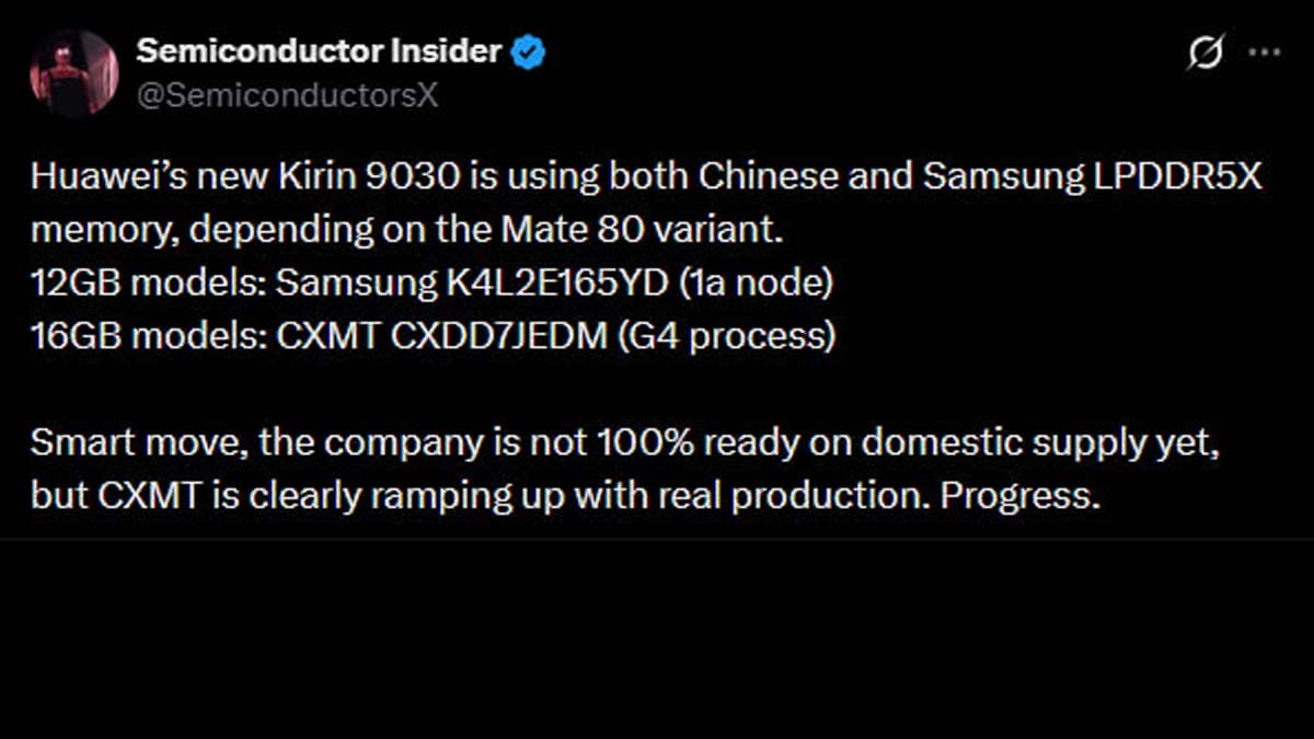
The finding that did not travel as fast was this: the 16GB Pro Max variants of the Mate 80 arrived at SemiAnalysis’s lab with two different memory packages. One carried Samsung LPDDR5X. The other carried CXMT. ChangXin Memory Technologies – the Hefei-based DRAM manufacturer that Beijing has spent the better part of three years and an estimated $10 billion building into a national champion – has made it into Huawei’s highest-tier consumer flagship. That is not a footnote. That is the story of the Kirin 9030.
The distinction matters because logic and memory have always been the two pillars of semiconductor self-sufficiency. China has been making credible if expensive progress on logic – SMIC’s N+3 being the latest evidence – for years. Memory has been the harder problem, the one where Samsung, SK Hynix and Micron have held structural advantages in yield, density and cost that domestic entrants have struggled to close. The CXMT package discovered in the Mate 80 Pro Max, marked CXDD7JEDM and assembled in week 45 of 2025, represents the clearest signal yet that Chinese memory is no longer an aspiration on a government roadmap. It is in the phone.
SemiAnalysis found that the 12GB variant of the Kirin 9030 Pro uses Samsung’s K4L2E165YD – LPDDR5X-9600 built on Samsung’s 1a node, the fourth generation of its 10-nanometer-class DRAM family. That chip has been in volume production since 2022, meaning Huawei’s flagship is running current Samsung memory, not old-node inventory. The irony of this is not lost on anyone tracking the geopolitics: a Chinese technology company blacklisted by the United States government is sourcing its premium memory tier from the flagship chip division of a South Korean company whose country actively participates in the export-control architecture designed to contain it.
The CXMT alternative fills the 16GB Pro Max tier. SemiAnalysis’s X-ray computed tomography analysis pegged the CXMT die dimensions as consistent with a density of roughly 0.3 gigabits per square millimeter – equivalent to the 1z-class nodes that Samsung and SK Hynix were running two or three years ago. That is a generational lag. But it is a commercially shipping generational lag inside a flagship device, which is a categorically different thing from a lab demonstration.
Against that backdrop, the SMIC N+3 process findings are still worth understanding on their own terms. Huawei’s approach to chip constraints has consistently been to treat architecture and packaging as a substitute for process headroom, and the Kirin 9030 shows both the gains and the limits of that strategy.
SMIC reached a transistor density of 113.4 million transistors per square millimeter on N+3, slightly above the 107.7 million on TSMC’s N6 – a mature node that entered volume production years ago and relies on extreme ultraviolet lithography for some layers. SMIC achieved comparable density using only deep ultraviolet equipment through a technique called self-aligned quadruple patterning at the M0 metal layer. To put that concretely: where TSMC needs two patterning passes on that layer, SMIC needs four. Each additional pass adds masks, overlay sensitivity and process risk. The transistor count lands in the same neighborhood. The manufacturing economics do not.
SemiAnalysis was direct about what this means. The American Enterprise Institute’s April 2026 analysis, published in its report on China’s lithography strategy, estimated SMIC’s 5-nanometer-class process costs 40 to 50 percent more than TSMC’s equivalent, with yields significantly below the benchmarks TSMC operates at. SMIC is printing chips that benchmark at a comparable density class. It is doing so at a structurally higher cost, which is a fact that matters enormously if you are Huawei trying to price a consumer smartphone.
On performance, the Kirin 9030 tells a two-speed story. The GPU made a genuine leap – the Maleoon 935 puts up 3DMark Wild Life Extreme scores roughly 70 percent above the previous Maleoon 920 and reaches approximately where Android flagships were in 2022 – competitive with the Snapdragon 8+ Gen 1, materially behind the Snapdragon 8 Elite Gen 5. The CPU is a harder read. SemiAnalysis’s benchmarks show the TaiShan Prime core running at instructions-per-clock roughly equivalent to Arm’s Cortex-X2, a 2021 design. Apple’s 2020 M1 Firestorm core holds a 35-percent per-clock advantage. The current Apple M5 P-core is approximately 2.7 times faster in absolute terms. The gap is not primarily Huawei’s design capability – the core design is genuinely competitive with the previous generation of leading-edge designs. The gap is the voltage-frequency curve that comes with N+3 versus TSMC N4 or N3P, which is what Apple, Qualcomm and MediaTek build on.
HiSilicon’s response to that constraint is LogicFolding, the 3D stacking roadmap that Huawei’s chip design arm unveiled at the ISCAS 2026 conference. The concept splits a single logic block across two active dies bonded face-to-face at ultra-fine pitch, shortening signal paths and recovering frequency from architecture rather than from transistor density. The roadmap targets a prime core frequency of 5 GHz by 2031, up from 2.75 GHz in the Kirin 9030; lab silicon at 3.39 GHz already exists according to Huawei. The density claim accompanying that roadmap – reaching 295 million transistors per square millimeter equivalent by 2031 – is where SemiAnalysis urges caution. Huawei is measuring density by package footprint across stacked active layers, a methodology that produces numbers not directly comparable to foundry-reported transistor density. Applying the same method to AMD’s MI450X, which stacks N2 and N3P dies, yields a theoretical 460 million transistors per square millimeter in 2026, well ahead of Huawei’s 2031 target under the same accounting.
What the SemiAnalysis teardown also revealed is that SMIC’s N+3 process knowledge is diffusing into the broader Chinese ecosystem. According to the report, SMIC is licensing its N+2 and N+3 processes to HLMC and Hua Hong at the direction of the central government. Design companies including Alibaba’s T-Head silicon unit and AI chip designer Cambricon are potential beneficiaries of that diffusion. The memory side shows a parallel dynamic: Chinese memory production is scaling aggressively, with a recent $1.86 billion domestic supply deal signaling the buildup in capacity. Export controls aimed at a single named company become structurally less effective once the underlying manufacturing knowledge has distributed across multiple fabs and design houses.
There is one thing the teardown cannot resolve: how long Huawei will need Samsung memory at the top of its lineup. The CXMT chip is two nodes behind in density terms. For a consumer flagship where the Pro Max sits at the premium tier, that gap creates real constraints on what memory configurations CXMT can support at competitive power and bandwidth. SemiAnalysis does not attempt to answer how quickly that closes. It is the question the next Kirin teardown will have to address.
In the meantime, the Kirin 9030 sits as evidence of exactly what sanctions policy can and cannot accomplish. They have not frozen Chinese semiconductor development. They have made it more expensive, more complicated and more dependent on architectural workarounds. Whether that is strategic success or strategic delay depends on a timeline that no one on either side of the Pacific has fully resolved.