
Huawei has unveiled one of the most ambitious semiconductor roadmaps in modern tech history, claiming it can achieve 1.4nm-class chip density by 2031 through a radical new engineering approach that bypasses traditional transistor scaling.
The Chinese technology giant introduced what it calls the “Tau (τ) Scaling Law” during the semiconductor symposium in Shanghai, presenting it as a successor to the slowing Moore’s Law era that has dominated chipmaking for decades.
At the center of Huawei’s strategy is a new architecture known as “LogicFolding,” which focuses on dramatically reducing signal propagation delays and shortening internal wiring paths inside processors rather than relying only on shrinking transistor sizes. Huawei says the approach can sustain performance gains even as physical and economic limitations make traditional chip scaling increasingly difficult.
The announcement is already sending shockwaves through the semiconductor industry because it directly targets one of the biggest weaknesses in China’s tech ambitions: the inability to access cutting-edge lithography systems due to US export restrictions.

Rather than trying to beat TSMC solely in fabrication technology, Huawei is pushing a system-level design philosophy that optimizes how data travels through chips and computing systems. According to the company, reducing communication delays can unlock major efficiency improvements without depending entirely on smaller process nodes.
Industry analysts view the move as a sign that China’s semiconductor race is evolving from manufacturing catch-up into architectural innovation.
Huawei claims its future Kirin processors arriving later in 2026 will become the first commercial chips built using the LogicFolding architecture. The company says the design substantially shortens internal chip wiring and boosts computational performance, especially for AI-related workloads. According to CNBC, the company’s strategy is increasingly aimed at challenging Nvidia’s dominance in China’s AI market.
The company also revealed it has already designed and mass-produced 381 chips over the past six years using technologies related to the Tau Scaling framework. Those chips have reportedly been deployed across smartphones, AI computing systems, and industrial applications.
Huawei’s timeline is especially aggressive.
The company says its architecture could eventually deliver transistor-density equivalence close to 1.4nm processes by 2031, a target that would place Huawei near the expected global frontier of semiconductor technology later this decade. Bloomberg noted that Huawei believes the approach could help shorten the gap with TSMC despite continuing sanctions.
That claim has triggered both excitement and skepticism across the tech world.
Huawei has not publicly released independent benchmark testing or technical validation for the Tau Scaling Law. Semiconductor experts caution that alternative architectures often face enormous challenges involving thermal management, software compatibility, manufacturing reliability, and production scalability. Independent analysts cautioned that the technology still faces years of real-world testing.
Still, the strategy aligns with a growing industry-wide realization that traditional scaling is approaching its practical limits.
For decades, Moore’s Law drove semiconductor progress by doubling transistor density approximately every two years. But as chips approach atomic-scale dimensions, the costs and technical difficulties of shrinking transistors further have exploded.
That reality has pushed chipmakers toward alternatives such as chiplets, 3D stacking, advanced packaging, and data-flow optimization. Huawei’s LogicFolding concept appears to combine several of those ideas into a broader framework designed to maximize computational efficiency.
The implications stretch far beyond smartphones.
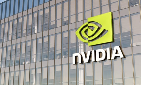
Huawei has rapidly transformed into China’s leading domestic challenger to Nvidia in AI infrastructure. Its Ascend AI processors are increasingly being adopted by Chinese cloud companies and enterprise customers looking for alternatives to restricted US hardware. The rise of Nvidia’s China AI ambitions has intensified the competition between American and Chinese semiconductor firms.
If Huawei succeeds in delivering meaningful performance gains without access to Western lithography tools, it could weaken one of the core assumptions behind US semiconductor sanctions.
The company’s resurgence has already surprised many observers.
After US restrictions crippled Huawei’s smartphone business several years ago, analysts widely believed the company would struggle to remain competitive in advanced semiconductor design. But Huawei stunned the industry with the return of high-end Kirin chips and domestically produced 5G smartphones, signaling that China’s chip ecosystem had progressed faster than expected.
Now Huawei is escalating its ambitions again.
Much of the momentum behind the company’s semiconductor revival has been driven by He Tingbo, the longtime Huawei executive often referred to in Chinese media as the company’s “chip queen.” A veteran engineer who helped build Huawei’s HiSilicon division into a major global semiconductor player, He presented the Tau Scaling Law during the ISCAS keynote in Shanghai.
Under her leadership, Huawei’s semiconductor arm has become one of China’s most strategically important technology programs.
The broader geopolitical stakes are impossible to ignore.
The United States has spent years trying to contain China’s access to advanced AI and semiconductor technologies, arguing that such systems have major military and national-security implications. China, meanwhile, has poured billions into domestic chip development to reduce dependence on foreign suppliers. The growing US-China semiconductor conflict is now reshaping the global technology industry.
Huawei’s latest announcement suggests the next phase of that battle may not be fought only through manufacturing capability, but through entirely new approaches to chip architecture and computing design.