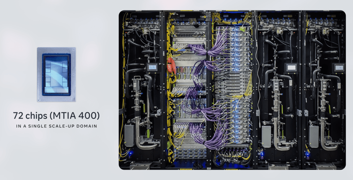

MENLO PARK — For most technology companies, a chip announcement is a carefully managed press release, calibrated for stock price and investor relations. For Meta, this month is different. Iris, the third chip under the company’s in-house MTIA program, has entered mass production at Taiwan Semiconductor Manufacturing Company’s most advanced facility, ending a years-long question about whether the world’s largest social media platform could actually build its own silicon at scale.
The chip cleared a six-week bug-testing phase without significant defects before entering the production queue. Iris was designed in partnership with Broadcom’s custom AI chip program, extended through 2029 under a multi-generation MTIA roadmap, and is manufactured on TSMC’s 3nm process, the same fabrication node used for the most advanced smartphone processors currently available.
The reason this matters is not that Iris replaces Nvidia’s GPUs. It doesn’t, and Meta’s AI capital expenditure guidance is explicit: the company’s H100 and B200 GPU fleet remains the backbone of its most demanding training infrastructure. What Iris changes is the ratio, and with it the leverage. Every inference workload running on Iris is one fewer GPU order. The recommendation engines that determine what four billion people see on Facebook and Instagram run inference billions of times per day. Custom silicon designed around those specific workloads, rather than general-purpose GPUs repurposed for the task, is both cheaper and more power-efficient at that scale.
Meta has been building toward this moment for years. The MTIA program began as an effort to reduce dependence on commodity GPUs for inference tasks, which means running a trained model as opposed to training it from scratch. Iris extends that mission considerably. Unlike its predecessors, it is designed to handle both large training runs and high-frequency inference simultaneously, making it Meta’s most versatile in-house chip yet.

To hit those targets, Meta has signed long-term supply agreements across the hardware stack: memory chips from Samsung Electronics, flash storage from Sandisk, and fiber-optic equipment from Sumitomo Electric. The Broadcom partnership, which now spans multiple chip generations, gives Meta a co-design partner that can translate its AI workload requirements directly into silicon, a capability that previously existed only inside Nvidia and AMD’s own engineering departments.
TechCrunch reported the production timeline in July after Reuters reviewed an internal company memo. The chip is designed to handle both the low-latency inference work that powers Meta’s consumer products and larger training runs, a dual role that earlier MTIA generations did not carry.
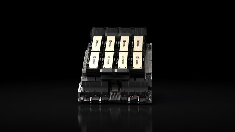
Nvidia’s data center chip business deserves harder scrutiny than it usually receives when custom silicon announcements land. The narrative that in-house chips threaten Nvidia’s business is real but overstated in the near term. The company’s data center revenue has continued to grow through every announced competitor. The more durable threat is structural: as Broadcom, Marvell, and others build co-design relationships with hyperscalers, the institutional knowledge of AI workload optimization accumulates outside Nvidia’s walls. That erosion is slower than any chip announcement implies, but it is directional.
The competitive context has tightened considerably this year. Huawei’s AI chip cluster demonstrated that advanced inference infrastructure can be assembled without access to Nvidia’s highest-end hardware, using homegrown accelerators built behind the manufacturing frontier. Meta’s Iris moves in a different direction, using the world’s most advanced foundry process rather than working around export restrictions. Both trajectories converge on the same conclusion: the era when a single chipmaker controlled the entire competitive landscape is already behind us.