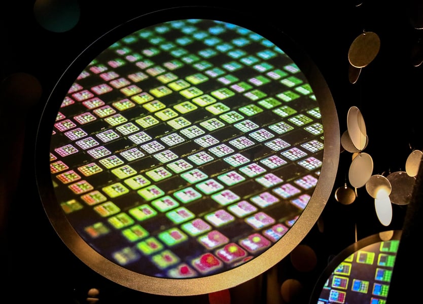
A TSMC semiconductor wafer on display at the TSMC Museum of Innovation in Hsinchu, Taiwan. Sony and TSMC are jointly investing $6.4 billion in a new image sensor plant in Kumamoto, Japan. [Image Source: TechCrunch / Bloomberg / Getty Images]
TOKYO – The camera in your next iPhone will almost certainly run on Sony silicon. So, in all probability, will the sensor behind the eye of the AI robot picking items from a warehouse shelf nearby.Sony and Taiwan Semiconductor Manufacturing Company said Monday they will build a second joint chip plant in Kumamoto, Japan, spending approximately $6.4 billion, or roughly ¥1 trillion, on a facility dedicated to image sensors, targeting mass production in 2029, Bloomberg reported. The announcement formalizes a bet the companies have been telegraphing for months: that the rapid expansion of physical AI, the term for AI systems embedded in cars, robots and industrial machinery, will create sensor demand that looks less like a modest upgrade cycle and more like an entirely new market.Sony holds roughly half the global market for image sensors, the chips that convert light into digital information. TSMC supplies the manufacturing muscle: Sony designs the sensor architecture, TSMC fabricates it, and the combination feeds into products ranging from iPhone camera modules to the lens systems deployed in Toyota driver-assistance systems. The new plant does not alter that arrangement. It deepens it.The demand argument that Sony and TSMC are making has three parts. The first is familiar. Apple’s iPhone cameras have required progressively faster, more capable image sensors with each generation; that specification race has been Sony’s primary growth engine for more than a decade. It continues.The second driver is automotive. Modern vehicles now incorporate multiple cameras for lane-keeping, blind-spot monitoring and, increasingly, more advanced driver assistance. The sensor count per vehicle has risen sharply, and the trend is far from finished.The third and most speculative demand driver is what the industry calls physical AI. AI systems embedded in machines that operate in physical space, including factory robots, delivery systems and household robots, need image sensors capable of high frame rates and wide dynamic range. Sony executives have said previously that this segment could eventually rival smartphones in sensor volume, which would be a large market if the projection proves accurate.
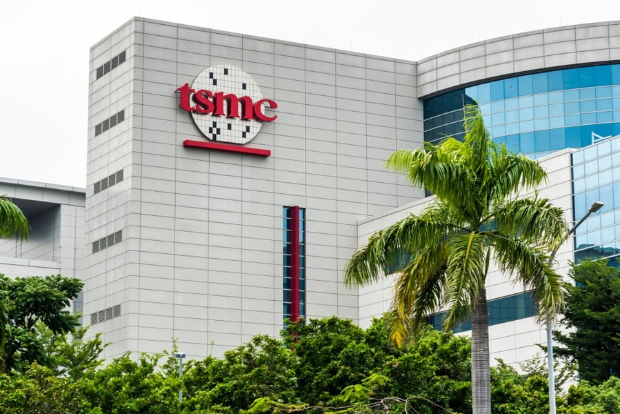
TSMC headquarters, Sony’s manufacturing partner for the $6.4 billion Kumamoto image sensor plant. [Image Source: TechCrunch / Getty Images]
Japan’s government has agreed to subsidize the project by approximately $380 million, continuing its effort to rebuild domestic chip manufacturing capacity. That effort centers increasingly on Kumamoto. TSMC’s chip manufacturing presence in Japan began with a joint venture called JASM, which started mass production in Kumamoto in 2025 and manufactures general logic chips. The Sony-TSMC image sensor facility will be a separate structure, operating in a different part of the chip market but benefiting from the regional infrastructure Japan has built around it.TSMC’s expansion elsewhere shows how broad its investment horizon has become. The company has pledged $265 billion for US manufacturing plants, positioning Kumamoto as one piece of a global production strategy. That diversification is deliberate: concentration risk in semiconductor supply chains has become a policy concern in Japan, the United States and Europe alike, and companies that depend on single-geography production have faced sustained political pressure to spread their footprint.No production capacity target for the Kumamoto image sensor plant has been publicly announced. That absence is notable. Semiconductor fabs announce wafer output targets when they want to signal scale to customers and investors; the omission suggests the specific numbers are either competitively sensitive or still being refined. The 2029 target for mass production gives the project roughly three years, which is tight for a greenfield facility of this complexity.Competition does not ease that pressure. Samsung has invested in imaging technology alongside its memory business and has image sensor products in the automotive market. Chinese chip companies, boosted by state subsidies, have been accelerating their development pace; while Sony’s position in the most advanced sensor nodes remains strong, the gap at mid-range specification levels has been narrowing.The Apple relationship is the clearest near-term anchor for the investment. Apple is not Sony’s only smartphone customer, but it sets the performance requirements that define what Sony has to build. When Apple specifies the sensor for the next iPhone camera system, Sony needs the capacity to deliver at the volumes Apple requires within a launch cycle that allows no slippage. A $6.4 billion plant is, among other things, insurance that Sony can keep saying yes.Physical AI is the investment that requires more patience. The market for AI-equipped robots operating in real environments is real and growing, but its exact trajectory over the three years before the Kumamoto plant opens is genuinely uncertain. Sony and TSMC are committing ¥1 trillion to a forecast they believe in but cannot guarantee. That is the nature of long-cycle semiconductor investment: the wrong call at this stage does not become visible until years later. Whether the demand materializes on the timeline both parties are counting on remains the open question that no announcement can resolve.
Synthia Rozario is a journalist at The Eastern Herald covering travel, entertainment, fashion, celebrity news, hospitality, casino and gambling, with a focus on developments across lifestyle, tourism and popular culture.