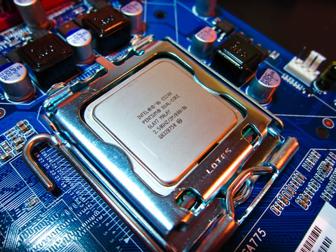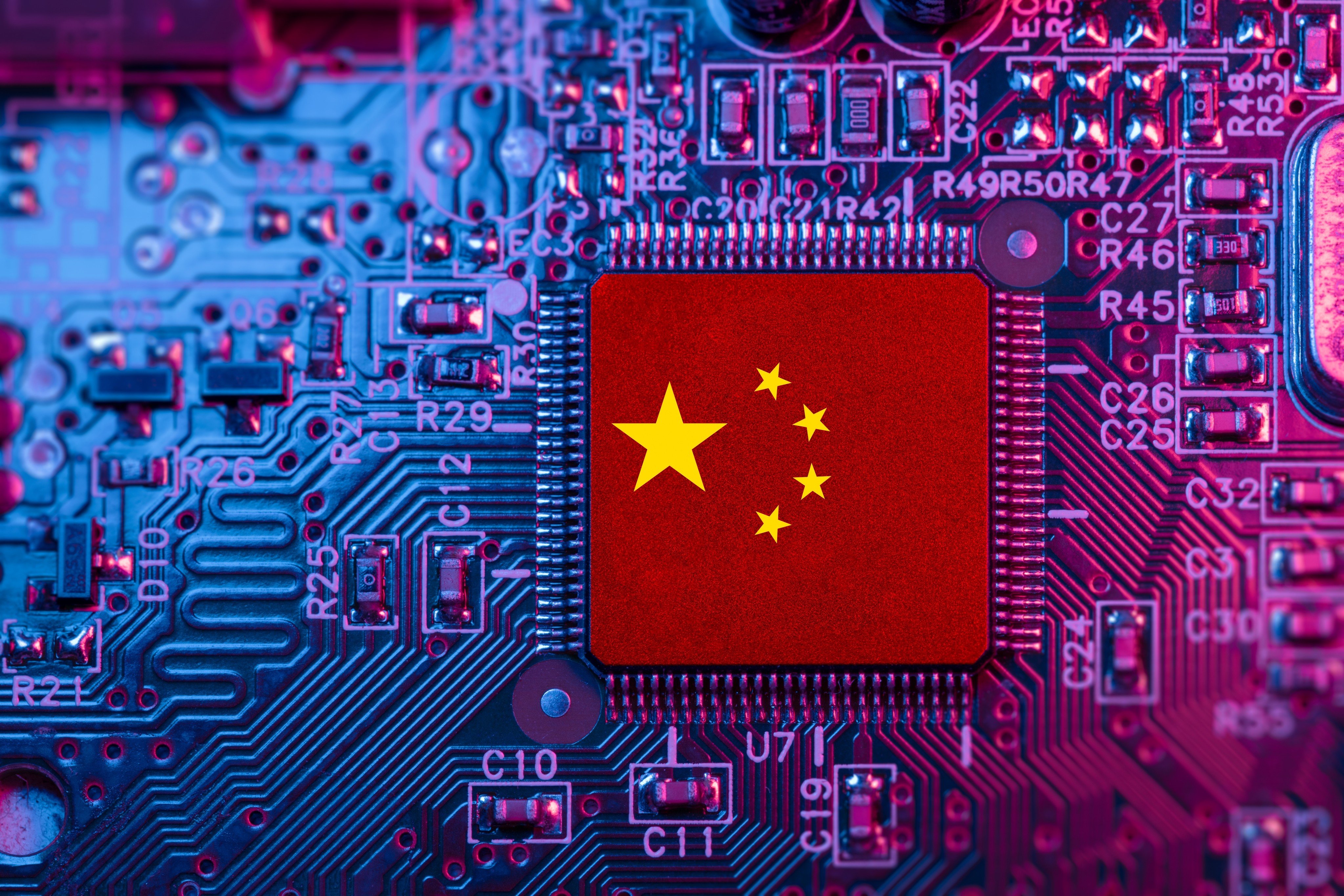

SHENZHEN, June 13, 2026 (The Eastern Herald) — China’s largest electronic design automation firms have moved this week to fall in behind Huawei’s Tau Scaling Law, the architectural framework the sanctions-walled chipmaker introduced last month and now wants the entire Chinese semiconductor stack to optimise around. Empyrean Technology, the country’s leading EDA vendor, unveiled Argus, a three-dimensional integrated circuit physical verification platform that the firm explicitly described as a key carrier for the new scaling principle. Peking University researchers, on the same day, released a prototype EDA tool built around what they called a true-3D approach compatible with Huawei’s LogicFolding architecture.
The Tau Scaling Law, presented in late May at the IEEE International Symposium on Circuits and Systems in Shanghai by Huawei’s chip queen He Tingbo, proposes to replace Moore’s Law on Chinese drawing boards. Where Moore’s framework chases ever-smaller transistors, Tau prioritises the time taken by a signal to cross a chip, and uses three-dimensional folding of logic blocks to shorten critical paths instead of relying on extreme-ultraviolet lithography to shrink them. The target is a transistor density equivalent to a 1.4-nanometer process, deliverable by 2031, with 55 percent higher density than current advanced nodes and without the EUV machinery that ASML is forbidden to export to China.
The peg this week is alignment. Huawei does not own a meaningful EDA franchise of its own and cannot reach the 2031 target on internal tooling alone. Empyrean and the smaller domestic EDA challengers, Primarius, Cellix and Semitronix, between them control roughly 17 percent of the Chinese EDA software market, with Cadence Design Systems, Synopsys and Siemens EDA carving up almost all of the remainder. The American and German trio have been progressively constrained from selling their most advanced flows into Huawei-linked design houses since 2022 and were tightened further in the latest BIS rule round in March. The Chinese tooling stack therefore has to deliver Tau, or Tau dies on the slide where it was drawn.
Beijing is helping the migration. The Ministry of Industry and Information Technology has redirected its national integrated-circuit fund priorities toward EDA software, packaging tools and 3D IC physical verification this fiscal year, and the State Council’s industry policy group set targets for replacing US EDA share inside state-funded fabs to 50 percent by 2028. The new five-year plan opening in 2027 is widely expected to enshrine the Tau framework, alongside CXL-style interconnect specifications, as a strategic standard. None of that guarantees the technical bet works. It does guarantee the political will is there.
The technical claim deserves the scepticism it is getting in the Western press. Tau Scaling and LogicFolding still need a leading-edge fabrication process to land 1.4-nanometer-equivalent density, even if that process is reached by a different route than Dutch EUV machines provide. SMIC’s most advanced production node is currently around 7-nanometer-class, achieved without EUV via multi-patterning on its DUV machines, and the gap to 1.4-nanometer-equivalent density is enormous. Huawei argues that gap shrinks dramatically if you measure by useful performance rather than transistor pitch alone, which is the conceptual move the Tau framework is trying to popularise.
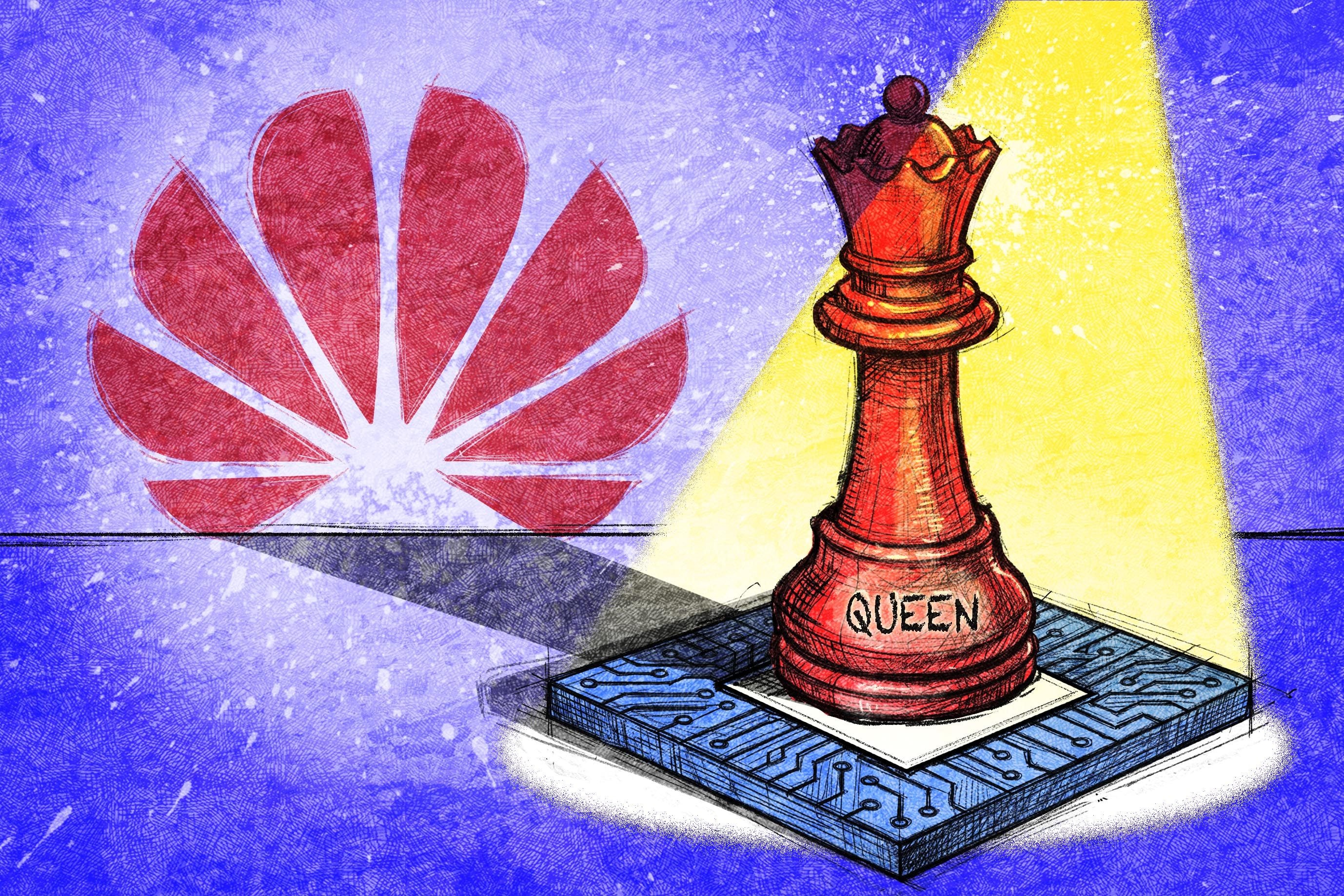
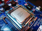
Some of the move is theatre, some is substance. Huawei says it has designed and mass-produced 381 chips over the past six years using the broader Tau-aligned design philosophy, including the Kirin smartphone application processors and Ascend AI accelerators that already power Chinese cloud AI deployments. The Kirin 9020-class chip scheduled for autumn 2026, expected to anchor the Mate 90 series, will be the first commercial silicon launching with LogicFolding inside. That is twelve months from announcement to commercial product, fast even by Shenzhen standards.
The political subtext is even louder than the technical one. The United States Commerce Department’s BIS has spent the last four years building a sanctions architecture aimed at slowing Chinese leading-edge chip development by ten to fifteen years. The Pentagon has gone further, adding Chinese tech firms to its 1260H list of designated military companies as recently as last week. Alibaba, BYD and Baidu were added in the most recent expansion, a signal that the United States is preparing the legal scaffolding for harsher restrictions even as the export-control system grows leakier. Tau is China’s answer to all of this. The argument is not that the lithography gap does not exist. It is that the gap is the wrong thing to measure.
Allies are being pulled into the slipstream as well. Taiwan is now in active consultation with Washington on how to extend the chip blockade further. Taipei is weighing curbs on its own AI-chip exports to mainland customers, including a possible ban on advanced-node TSMC sales to second-tier Chinese buyers identified by US intelligence as Huawei fronts. Europe is moving in fits. The Netherlands’ coalition has resisted further EUV restrictions for fear of ASML’s order book, and the European Chips Act funding remains stuck in member-state distribution wrangles. NATO is asking its members to remove existing Huawei equipment but US ambassador Matthew Whitaker warned this week that several allies remain too close to the Shenzhen group’s network gear.
Markets have priced the China-EDA realignment cautiously. Empyrean’s Shenzhen-listed shares have risen 38 percent this quarter, Cadence and Synopsys are flat in New York with their China-exposed revenue forecasts trimmed, and ASML’s stock has not moved meaningfully on the news because investors continue to assume that Chinese workarounds, however clever, still need some leading-edge equipment over the long run. The financial signal is roughly correct. Tau buys China time, options and political cover. It does not buy China parity overnight, and the chip queen’s own slides did not claim that it would.
What it does change is the framing. For the last decade, the United States enjoyed a narrative monopoly on what constituted advanced semiconductor progress, captured in three-letter shorthand from 7-nanometer down to 2-nanometer-class nodes. Tau is an attempt to break that monopoly with a different vocabulary, and the fact that Chinese EDA firms are now publicly architecting their tooling around the new vocabulary changes the geometry of the chip war. The South China Morning Post framed the alignment as a domestic catching-up moment with US rivals. Read from Shenzhen, it is something more ambitious, an attempt to relocate the centre of the technical conversation.
The 2031 target is not the end of the story. Huawei’s own technical announcement sets out a roadmap that runs to 2035 and includes optical interconnects, 3D stacked memory and silicon-photonics hybrids that bring the chip closer to a system-level rather than transistor-level competition. If the Tau framework delivers anything close to what is on the slides, the US export-control system that was built to slow Chinese leading-edge silicon by chasing transistor pitch will increasingly find itself chasing a problem the Chinese have stopped defining the same way.
For now the safer call is the boring one. China has chosen its angle and started to standardise on it. The United States has chosen its angle and started to harden it. Between the two, ASML keeps shipping DUV, Cadence keeps shipping EDA flows everywhere not legally fenced off, and the next genuinely informative milestone will be silicon. The Kirin 9020 inside the Mate 90 this autumn is the first real test. The financial markets, the export-control regime and the broader Chinese industrial story that has remade autos and clean energy are watching the same logic apply now to chips.