
HEFEI — The chip was expected to take longer to arrive.
When Washington barred ASML from shipping extreme-ultraviolet lithography machines to Chinese foundries three years ago, the policy rested on a clear assumption: without EUV, China’s memory manufacturers could not produce the leading-edge DRAM used in flagship smartphones.
On Saturday at the World Manufacturing Convention in Hefei, ChangXin Memory Technologies challenged that assumption. CXMT said its fifth-generation G5 DRAM process had entered mass production, with two 24-gigabit LPDDR5X products already shipping in Chinese flagship phones.
The company said the process achieves an 11.95-nanometer active-area half-pitch without EUV. Instead, it uses quadruple patterning: four precisely aligned photolithographic exposures that inscribe circuit features the restricted equipment would otherwise produce in a single pass.
The result is a manufacturing workaround that turns the export-control premise into a more complicated question: whether restricting access to the most advanced tools can delay Chinese progress without ultimately preventing it.
“Our process capability is now on par with the most advanced mass-produced nodes out there in the industry,” CXMT Vice President Luo Xiaodong said at the convention.
That statement carries a qualifier worth noting. CXMT produced that claim at a Chinese government-organized industrial forum in its home city, before an audience of domestic supply chain partners and state-backed investors. Independent process benchmarking by outside foundries or research institutions has not confirmed the comparison. The die yield figure CXMT disclosed, a claimed 50 percent improvement in gross dies per wafer versus its fourth-generation process, also comes from company disclosure rather than an independent manufacturing audit.
The caveat matters less on the domestic side. Chinese smartphone brands integrating CXMT’s LPDDR5X are not waiting for an independent process comparison before shipping handsets. The phones are already in production. The output is real.
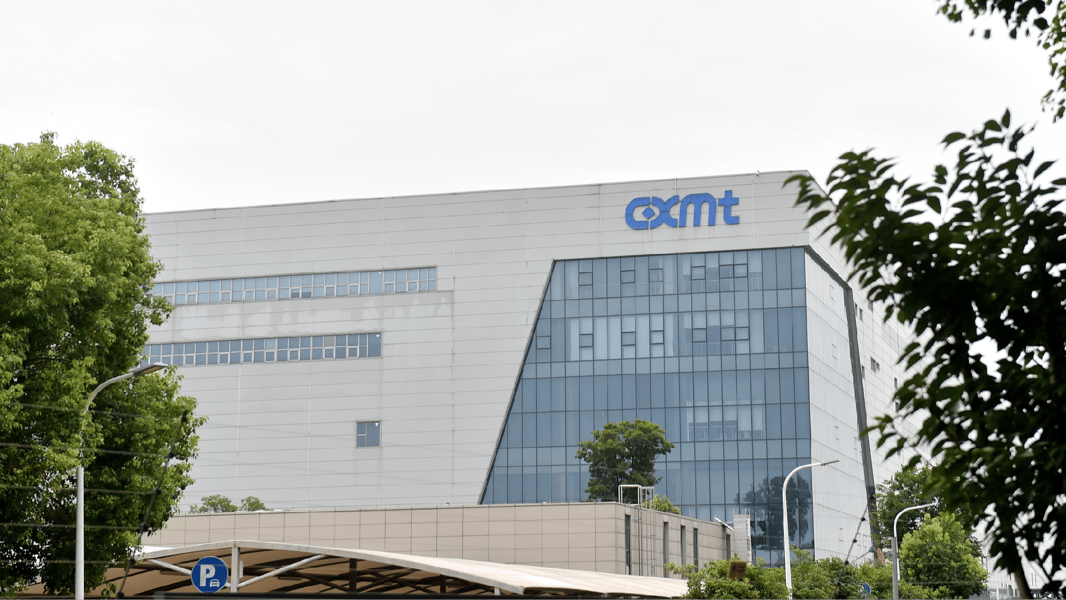
Capacity is CXMT’s clearest verifiable metric. The company currently operates at roughly 300,000 12-inch wafers per month across its facilities in Hefei and Beijing, and is targeting 350,000 to 375,000 by year-end 2026. That output, if achieved at the yields CXMT claims, translates into a production volume that Samsung and SK Hynix cannot ignore in mid-range LPDDR pricing.
The quadruple patterning method is worth understanding for what it is and what it is not. EUV produces fine circuit features using 13.5-nanometre wavelength light in a single exposure, which means fast throughput and fewer opportunities for alignment error to accumulate. DUV quadruple patterning reaches comparable feature dimensions through four aligned exposures, each carrying a small probability of misalignment. At sub-12-nanometre dimensions, accumulated misalignment is catastrophic. CXMT’s reported yield improvement implies its engineers have solved or sufficiently mitigated that alignment problem, a genuine process control achievement if confirmed, and a figure worth watching across several quarterly disclosures.
The G5 announcement does not position CXMT at the frontier of the DRAM hierarchy. Samsung’s sixth-generation process development is ongoing. SK Hynix’s HBM3E stack, which powers the majority of AI training infrastructure currently deployed, sits on a product roadmap that CXMT has not published an equivalent for. The gap at the leading edge has not closed. What the G5 announcement suggests is that the gap has stopped widening, with the DUV workaround strategy that US officials described as a measure that would exhaust itself as feature sizes shrank proving viable at 11.95 nanometres.
EH has followed CXMT memory appearing in Huawei teardowns and China’s semiconductor export surge through August 2026. The G5 platform is the clearest evidence yet that Chinese memory manufacturing has moved past a threshold. What it will look like in two years, and whether export controls tighten further or fracture along geopolitical lines, remains genuinely unresolved.